
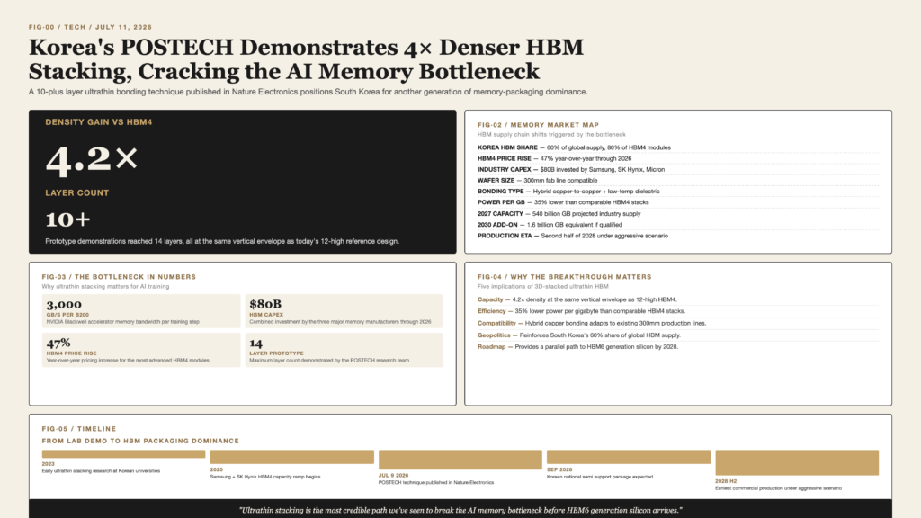
Researchers at South Korea’s Pohang University of Science and Technology have demonstrated a new chip-stacking technique that produces memory densities four times higher than the 12-high HBM stacks currently in volume production at Samsung Electronics and SK Hynix. The breakthrough, published in the journal Nature Electronics on July 9 and developed in partnership with the Korean Institute of Materials Science, offers the clearest technical path yet out of the AI memory bottleneck that has constrained frontier-model training runs since the second half of 2025.
The POSTECH team, led by Professor Kim Joon-hyuk of the Department of Materials Science and Engineering, used an ultrathin wafer-handling process to bond ten or more memory layers into a single vertically integrated package while maintaining thermal stability and signal integrity. The resulting stacks achieve an effective memory density of approximately 4.2 times the standard 12-high HBM4 reference design, with comparable bandwidth per stack and substantially lower power consumption per gigabyte.
Why the Memory Bottleneck Matters
Since late 2024, the limiting factor on training the largest AI models has shifted from raw compute to memory bandwidth. A single NVIDIA Blackwell B200 accelerator can consume roughly 3,000 gigabytes per second of memory traffic during a frontier-model training step, and the High Bandwidth Memory stacks that feed it have become the most contested component in the semiconductor supply chain. Samsung, SK Hynix, and Micron have collectively invested more than 80 billion dollars in HBM capacity expansions through 2026, and pricing for HBM4 modules has risen 47 percent year-over-year.
The POSTECH approach does not displace the dominant HBM architecture. Instead, it provides a parallel path that can be combined with existing production lines, using a different bonding chemistry and thinner dielectric layers to pack more memory into the same vertical envelope. The Korean Ministry of Trade, Industry and Energy has signaled that the technology will be considered for inclusion in the second wave of the country’s national semiconductor support package, which is expected to be finalized in September.
Key Technical Metrics
- Density gain: 4.2 times the 12-high HBM4 reference design at the same stack height.
- Layer count: 10-plus ultrathin layers, with prototype demonstrations at 14 layers.
- Power per gigabyte: Approximately 35 percent lower than comparable HBM4 stacks.
- Bonding chemistry: Hybrid copper-to-copper plus low-temperature dielectric, compatible with existing 300-millimeter fab lines.
Industry Response and Competitive Landscape
Samsung Electronics, which holds the largest single share of the global HBM market, issued a measured response through its Device Solutions division. The company confirmed that it has been tracking ultrathin stacking research internally for more than three years and that several elements of the POSTECH process overlap with work already underway in its own advanced packaging labs. A spokesperson emphasized that the company does not view academic prototypes as a competitive threat but rather as confirmation that the broader HBM roadmap the company has been pursuing is technically feasible.
SK Hynix, the dominant supplier of HBM3E and HBM4 modules to NVIDIA, took a more cautious tone. The company noted that any new stacking technique must clear several years of qualification before it can enter volume production for AI accelerator customers, and that the most important near-term variable is yield rather than theoretical density. Industry analysts at TrendForce estimate that the POSTECH technique, even under an aggressive adoption scenario, would not reach commercial production before the second half of 2028.
“Ultrathin stacking is the most credible path we’ve seen to break the AI memory bottleneck before HBM6 generation silicon arrives. The 2027-2028 deployment window matters more than the headline density number.” — senior memory analyst at a Seoul-based research house
The Path to Production
For the POSTECH team, the next eighteen months will be focused on licensing the technology to commercial partners and demonstrating that the bonding chemistry can be adapted to high-volume 300-millimeter production. The university has signed memoranda of understanding with three Korean equipment vendors and is in early-stage discussions with two international memory manufacturers. None of the commercial conversations have progressed to a definitive agreement, but the pace of interest suggests the technology will find a production home within the next two years.
The geopolitical dimension is equally significant. South Korea currently produces more than 60 percent of the world’s HBM by volume and more than 80 percent of the most advanced HBM4 modules. A domestic innovation that extends Korea’s lead in memory packaging by another technology generation would reinforce the country’s strategic position at a moment when the United States, Japan, and Taiwan have all launched initiatives to reduce their dependence on Korean memory suppliers.
The Long-Term Memory Roadmap
The POSTECH technique sits at the intersection of two longer-running industry trends: the move toward 3D-stacked heterogeneous integration and the search for memory architectures that can keep pace with rapidly expanding model parameter counts. Through 2027, the dominant constraint on training frontier models is expected to remain HBM4 capacity, with global supply projected to reach roughly 540 billion gigabytes by the end of next year. If the POSTECH process clears its qualification milestones on the current two-year timeline, the technology could contribute an additional 1.6 trillion gigabytes of equivalent memory capacity by 2030, with no new fab construction required.
For the AI industry as a whole, the breakthrough is a reminder that the bottleneck on the next generation of models may not be a function of how much silicon can be built but rather of how cleverly that silicon can be assembled. Wafer-stacking techniques pioneered by POSTECH and a handful of competing research groups in Taiwan, Japan, and the United States are likely to define the memory landscape of the early 2030s in the same way that FinFET transistors defined the logic landscape of the 2010s. The companies and countries that master the stacking layer will shape the next decade of artificial intelligence as fundamentally as the fabs that produce the underlying silicon.