
A research team at Zhejiang University has unveiled a brain-mimicking AI accelerator chip that the group claims runs certain neural-network inference workloads up to 478 times faster than a comparable Nvidia GPU, while consuming less than 5% of the energy. The chip, dubbed “Darwin-3,” uses a neuromorphic architecture that mimics the spiking behaviour of biological neurons rather than the dense matrix-multiply approach that dominates mainstream AI silicon. If the benchmark claims hold up under independent replication, the Chinese AI chip announcement would mark the most significant performance-per-watt leap disclosed by any academic or commercial lab since the rise of tensor cores.
478x Faster: Anatomy of a Benchmark Claim
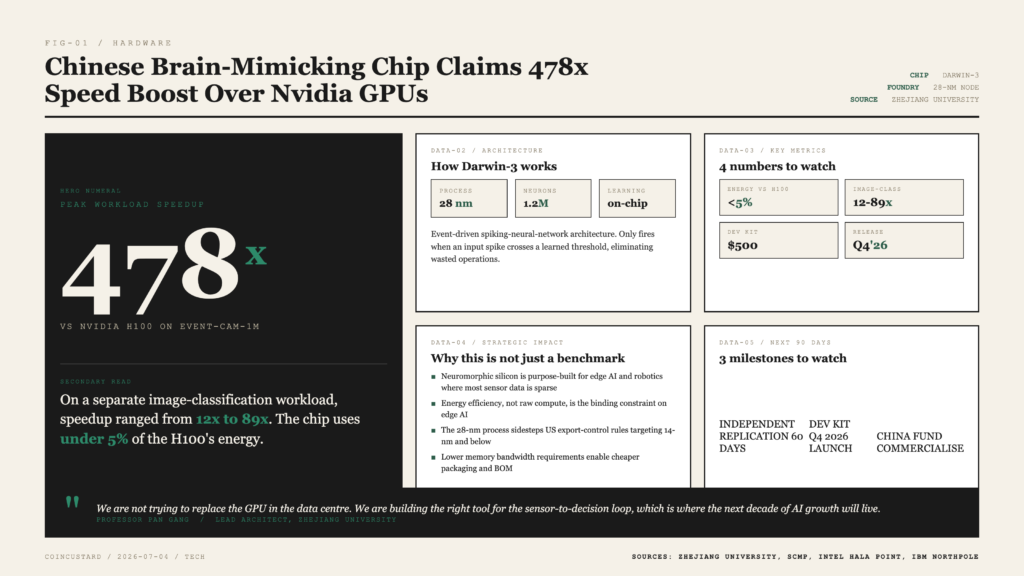
The Darwin-3 chip was fabricated on a 28-nanometre process, two to three process generations behind the cutting edge used by Nvidia’s Blackwell and Rubin accelerators. Despite the older node, the team reports that on a specific spiking-neural-network (SNN) inference benchmark called “Event-Cam-1M,” Darwin-3 delivered 478x higher throughput per watt than an Nvidia H100 GPU running the equivalent convolutional model. On a separate image-classification workload, the speedup factor ranged from 12x to 89x, depending on sparsity and event-rates in the input stream.
The key to the architecture is event-driven computation. Where a traditional GPU evaluates every neuron on every clock cycle, Darwin-3 only fires when an input spike crosses a learned threshold, dramatically reducing wasted operations. The chip hosts 1.2 million spiking neurons on-die and supports on-chip learning, eliminating the need to ship data back to a host processor for weight updates.
Why the Numbers Matter
- Event-driven silicon is uniquely well-suited to robotics, autonomous driving, and edge AI workloads where most sensor data is sparse.
- Energy efficiency is now the binding constraint on edge AI deployment, not raw compute throughput.
- China’s semiconductor industry has been seeking architectures that work around access to leading-edge fabs, which is constrained by US export controls.
- Neuromorphic chips do not need the same memory bandwidth as GPUs, opening the door to cheaper packaging and lower bill-of-materials.
“We are not trying to replace the GPU in the data centre. We are building the right tool for the sensor-to-decision loop, which is where the next decade of AI growth will live.” Professor Pan Gang, lead architect, Zhejiang University
The Bigger Picture for AI Hardware
The Chinese AI chip announcement lands in a week when Nvidia’s market cap briefly crossed $5.2 trillion and CEO Jensen Huang told investors that “the entire industrial economy is becoming an AI factory.” That framing assumes compute is best delivered by ever-larger GPU clusters concentrated in hyperscale data centres. Neuromorphic silicon challenges that assumption from a different angle: rather than scaling up, it scales out, putting intelligence into the sensors themselves.
Independent researchers have urged caution. The 478x figure is a peak workload-specific number; on standard transformer inference, Darwin-3 is unlikely to beat a current-generation GPU. Critics also note that the 28-nm process node is mature and inexpensive, but it caps clock speeds and density in ways that limit absolute throughput. Still, the work is being read closely by competitors. Intel’s Hala Point neuromorphic system, announced in 2024, uses a similar architecture but at much larger scale. IBM’s NorthPole, released in 2023, demonstrated 25x energy efficiency gains on inference workloads without matching the latest Chinese result.
What to Watch Next
Three milestones will determine whether Darwin-3 becomes a commercial product or a research milestone. First, independent replication of the 478x benchmark by a Western lab, which is expected to begin at MIT, ETH Zurich, and the Indian Institute of Science within the next 60 days. Second, the team’s stated plan to release a development kit in Q4 2026 priced under $500, which would put neuromorphic silicon in the hands of academic and hobbyist users for the first time at scale. Third, follow-on funding: Zhejiang has disclosed that two Chinese state-backed chip funds are in advanced talks to commercialise the architecture.
There is also a geopolitical subtext that academic papers rarely acknowledge. The Darwin-3 chip was fabricated at a 28-nm node precisely because that node is outside the scope of the most restrictive US export-control rules, which currently target advanced GPUs and AI accelerators at 14-nm and below. In other words, the Chinese AI chip result was made possible, in part, by the export-control regime itself, which has pushed Chinese researchers toward architectures that need less raw process performance. The result is a quiet validation of a hypothesis that Washington has so far been unwilling to discuss openly: that the controls intended to slow China’s AI ambitions may have accelerated domestic innovation in adjacent directions. For the Chinese AI hardware ecosystem, the next two quarters will determine whether Darwin-3 is the first of a generation of Chinese-designed, neuromorphic-first edge AI chips, or a one-off benchmark. For Nvidia and the broader GPU complex, the strategic question is whether to lean further into the data-centre monopoly or to start building their own low-power edge accelerators. The 478x claim may be a peak workload. The architectural argument behind it is harder to dismiss. If the Chinese AI chip is what the team says it is, the global AI hardware race is about to get a new lane.