
IBM Unveils World’s First Sub-1 Nanometer Chip, Redefining Semiconductor Roadmap
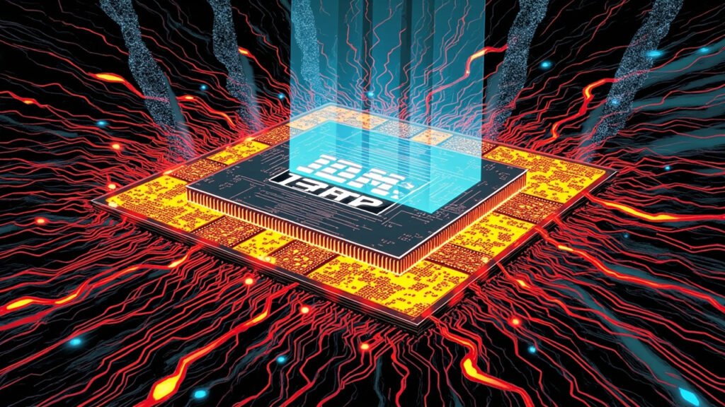
IBM has announced what it calls the world’s first sub-1 nanometer chip technology, a breakthrough that pushes semiconductor manufacturing into territory previously thought to be years away and could reshape the competitive dynamics of the global chip industry. The announcement, made from IBM’s research lab in Albany, New York, describes a new chip architecture that the company says packs more than 100 billion transistors onto a single chip using a stacked nanosheet design that breaks through the conventional limits of silicon scaling.
The new chip, which IBM is branding under the “nanostack” name, achieves its density by stacking transistors vertically rather than spreading them across a single plane, allowing the company to effectively shrink the gate length to less than one nanometer without requiring the expensive and difficult transition to exotic new materials. The breakthrough could give IBM and its manufacturing partners a multi-year lead in the race to build the next generation of AI accelerators and high-performance computing chips.
Why Sub-1 Nanometer Matters
For decades, the semiconductor industry has ridden Moore’s Law, doubling transistor density roughly every two years by shrinking the smallest features on a chip. That progress has stalled in recent years as traditional 2D scaling approaches fundamental physical limits, prompting chipmakers to invest billions in new materials, new architectures, and entirely new manufacturing techniques. IBM’s vertical stacking approach sidesteps many of those challenges by reusing existing fabrication infrastructure while delivering density gains that would otherwise require a leap to new transistor geometries.
The Vertical Stacking Breakthrough
The new architecture uses a multi-layer nanosheet design in which transistor layers are stacked directly on top of one another. This vertical integration allows for significantly higher transistor density per unit area, while also reducing the distance that electrical signals need to travel between transistors. Shorter signal paths mean faster switching speeds and lower power consumption, both critical metrics for AI workloads that demand enormous computational throughput.
- More than 100 billion transistors packed onto a single chip
- Sub-1 nanometer effective gate length via vertical nanosheet stacking
- Significant improvements in performance per watt versus planar designs
- Compatible with existing fabrication infrastructure, easing adoption
- Targeting AI accelerators, high-performance computing, and mobile applications
“This is not just an incremental improvement. It is a fundamentally new way of thinking about how transistors are arranged on a chip,” said an IBM Research spokesperson. “We believe this approach will define the next decade of semiconductor innovation.”
Implications for the Chip Industry
The announcement lands at a delicate moment for the global chip industry. TSMC, Samsung, and Intel have all invested heavily in their own sub-2 nanometer processes, with production slated to begin in 2027 and 2028. IBM’s breakthrough, if it can be commercialized, would leapfrog those efforts and give IBM and its manufacturing partners a significant time-to-market advantage. The company is reportedly in discussions with several major foundries about licensing the technology, though it has not yet announced a formal partner.
Beyond the competitive implications, the breakthrough could also reshape the economics of advanced chip manufacturing. By enabling sub-1 nanometer densities without requiring entirely new fabrication equipment, the technology could lower the capital expenditure required to build next-generation fabs, potentially opening the door for new entrants and reducing the industry’s reliance on a small number of leading-edge manufacturers.
The AI Connection
It is no coincidence that IBM chose to highlight AI workloads in its announcement. The demand for AI accelerators has exploded over the past three years, with companies like NVIDIA, AMD, and a growing list of custom silicon providers competing to deliver the most powerful training and inference chips. Higher transistor density directly translates into more compute per chip, which in turn enables larger AI models, faster training times, and more efficient inference deployments.
Beyond Traditional AI Accelerators
The new architecture is also expected to benefit a wide range of applications beyond AI, including scientific simulation, cryptography, and high-frequency trading. The performance-per-watt improvements are particularly important for data center workloads, where power and cooling constraints increasingly limit how much compute can be packed into a single rack. By reducing the power required per transistor, the new design could enable denser server configurations and lower total cost of ownership.
Roadmap to Commercialization
IBM has a long history of pioneering semiconductor breakthroughs that the industry eventually adopts at scale. The company’s prior innovations, including the first 7nm and 5nm test chips, were eventually commercialized through partnerships with Samsung and other manufacturers. The new sub-1 nanometer architecture is expected to follow a similar path, with production-scale manufacturing likely to begin in 2028 or 2029.
Competitive Response Expected
TSMC and Samsung are both likely to accelerate their own research into vertical transistor stacking in response to IBM’s announcement. Intel, which has been working on its own sub-2 nanometer processes, may also need to reassess its roadmap in light of the new density benchmark. The next 18 months are likely to see a flurry of announcements as the major players respond to IBM’s lead and jockey for position in the next generation of semiconductor manufacturing.
The Bigger Picture
IBM’s sub-1 nanometer breakthrough is more than just a technical milestone. It is a signal that the semiconductor industry still has room to innovate even as the easy gains from traditional scaling have been exhausted. By combining creative architectural thinking with practical manufacturing compatibility, IBM has opened a new chapter in the long history of chip design. For the broader technology ecosystem, from cloud providers to AI startups, the announcement is a reminder that the underlying hardware powering the AI revolution continues to evolve in ways that could reshape what is computationally possible in the years ahead.